


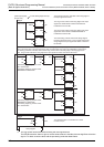
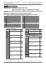
35 Interrupt Function and Pulse Catch Function
816
FXCPU Structured Programming Manual
[Basic & Applied Instruction]
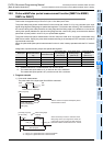
35.8 Pulse width/Pulse period measurement function [M8075 to M8083, D8074 to D8097]
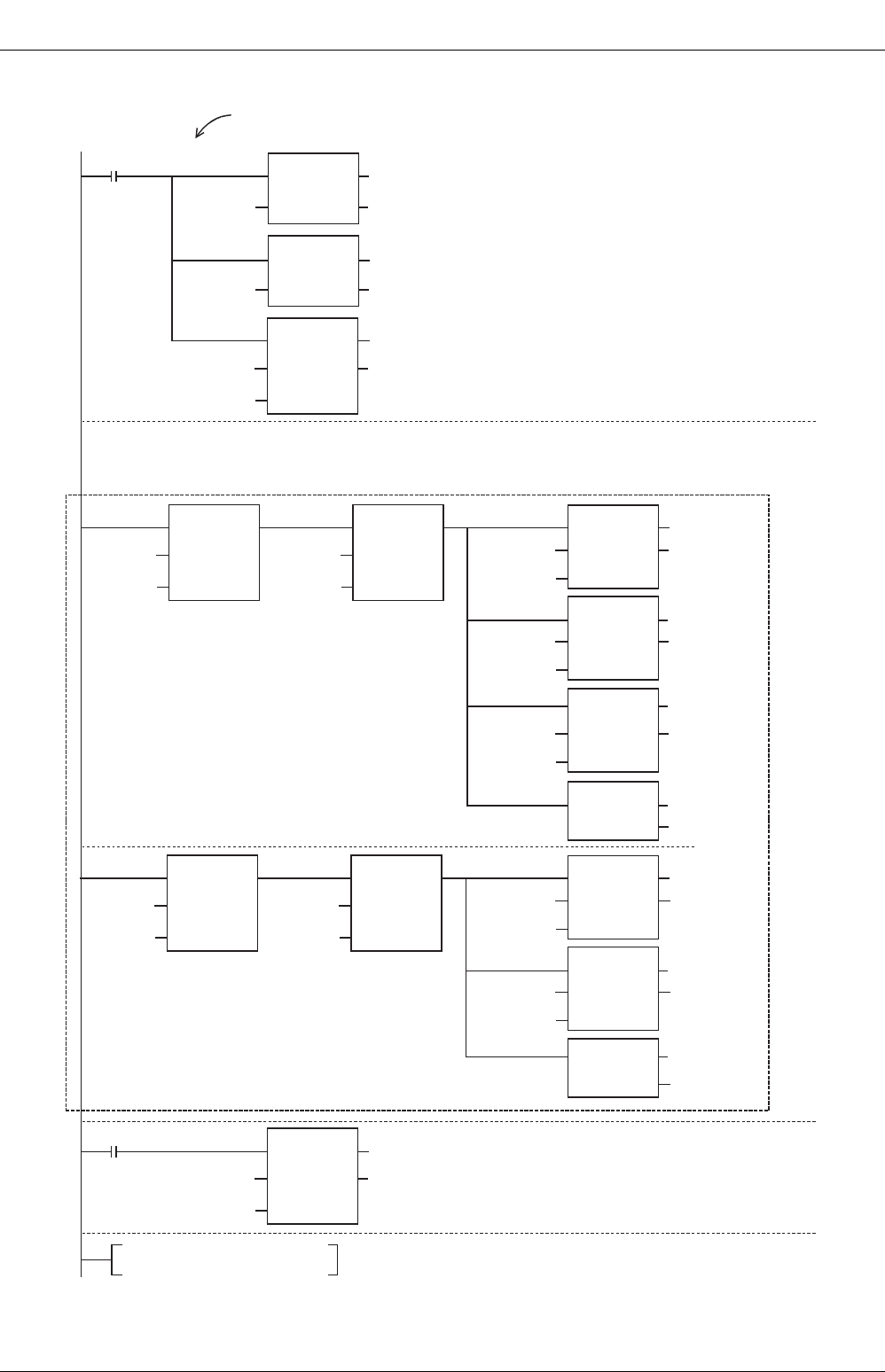
*1. The ring counter offers 32-bit data including the most significant bit.
The DSUB instruction does not give a correct value because it handles the most significant bit as the
sign bit. To obtain a correct value, add the processing inside the dotted frame.
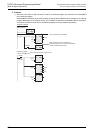
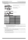
The ring counter value at the rising edge of the input
signal from X000 stored in D8074 and D8075 is
transferred to D1 and D0.
The ring counter value at the rising edge of the input
signal from X001 stored in D8080 and D8081 is
transferred to D3 and D2.
The value "Ring counter value at the rising edge of
the input signal from X001 - Ring counter value at the
rising edge of the input signal from X000" is stored in
D9 and D8.
X000 Rising edge ring counter value:
H0 to H7FFFFFFF
X001 Rising edge ring counter value:
H80000000 to HFFFFFFFF
X000 Rising edge ring counter value:
H80000000 to HFFFFFFFF
X001 Rising edge ring counter value:
H0 to H7FFFFFFF
The obtained value is converted into a value
in units of 10 μs.
When either one between the ring counter value at the rising edge of the input signal from X000 and the ring counter
value at the rising edge of the input signal from X001 is located within the range from H80000000 to HFFFFFFFF,
the following process is executed, and the value "Ring counter value at the rising edge of the input signal from
X001 - Ring counter value at the rising edge of the input signal from X000" is stored in D9 and D8
*1
.
The interrupt routine is executed at the rising edge of
the input signal from X001.
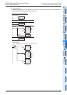
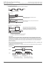
[Interrupt program]
(Event: I101)
X001 Rising edge interrupt
DMOV
M8000
RUN monitor
D8074 D0
EN ENO
sd
DINC
D8
EN ENO
d
DMOV
D8080 D2
EN ENO
sd
DSUB
D2 D8
EN ENO
s1 d
D0
s2
DSUB
H7FFFFFFF D4
EN ENO
s1 d
D0
s2
DSUB
D2 D6
EN ENO
s1 d
H80000000
s2
DADD
D4 D8
EN ENO
s1 d
D6
s2
LDD>=
D0
EN ENO
s1
K0
s2
ANDD<
D2
EN ENO
s1
K0
s2
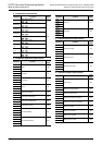
DINC
D8
EN ENO
d
DSUB
HFFFFFFFF D4
EN ENO
s1 d
D0
s2
DSUB
D2 D8
EN ENO
s1 d
D4
s2
LDD<
D0
EN ENO
s1
K0
s2
ANDD>=
D2
EN ENO
s1
K0
s2
M8000
DDIV
D8 D10
EN ENO
s1 d
K60
s2
User program