15 Applied Instructions (External Device (optional device))
15.6 VRRD / Volume Read
408
FXCPU Structured Programming Manual
[Basic & Applied Instruction]
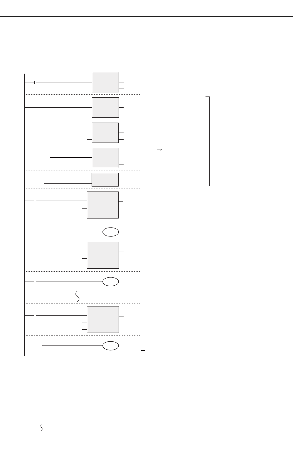
Program example
Variable resistor values are read out sequentially.
Depending on variable resistors VR0 to VR7, the specified values of VRRD instruction are K0 to K7.
In the example below, being decorated by index (Z = 0 to 7), K0Z is K0 to K7.
TS0
Y000
OUT_T
EN
TCoil
TValue
ENO
TC0
D200
M8000
Z
FOR
EN
n
ENO
K8
M8000
VRRD
EN
s
ENO
d
K0Z
D200Z
INC
EN ENO
d
Z
NEXT
EN ENO
X000
OUT_T
EN
TCoil
TValue
ENO
TC1
D201
X001
TS1
Y001
OUT_T
EN
TCoil
TValue
ENO
TC7
D207
X007
TS7
Y007
(Z)+1
RST
EN ENO
d
[ ST ]
RST(M8000, Z);
FOR(TRUE, K8);
VRRD(M8000, K0Z, D200Z);
INC(M8000, Z);
NEXT(TRUE);
OUT_T(X000, TC0, D200);
OUT(TS0, Y000);
OUT_T(X001, TC1, D201);
OUT(TS1, Y001);
OUT_T(X007, TC7, D207);
OUT(TS7, Y007);
[Structured ladder/FBD]
Reset of index register
(Z) = 0
FOR instruction is repeated 8 time
s
as specified.
In this period, the value of index
register Z is increased sequentially
from 0 to 1, 2, ..., 7, and the value
is transferred 8 times, from VR0 to
D200, VR1 to D201,..., VR7 to D20
Range of FOR to NEXT is
repeated 8 times.
Variable resistor value is
stored in data register.
This is a timer circuit.
Depending on graduations 0 to 10 of
the variable resistor, values of 0 to
255 are stored in the data register.
T0 to T7 are 100 ms timers, and 0 to
25.5 sec are obtained corresponding
to the set values of 0 to 255.
RUN monitor
(Z)


