


5 Basic Instruction
5.2 LDP, LDF, ANDP, ANDF, ORP, ORF
59
FXCPU Structured Programming Manual
[Basic & Applied Instruction]
1
Outline
2
Instruction List
3
Configuration of
Instruction
4
How to Read
Explanation of
Instructions
5
Basic Instruction
6
Step Ladder
Instructions
7
Applied Instructions
(Program Flow)
8
Applied Instructions
(Move and
Compare)
9
Applied Instructions
(Arithmetic and
Logical Operation)
10
Applied Instructions
(Rotation and
Shift Operation)
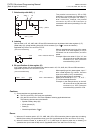
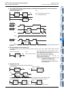
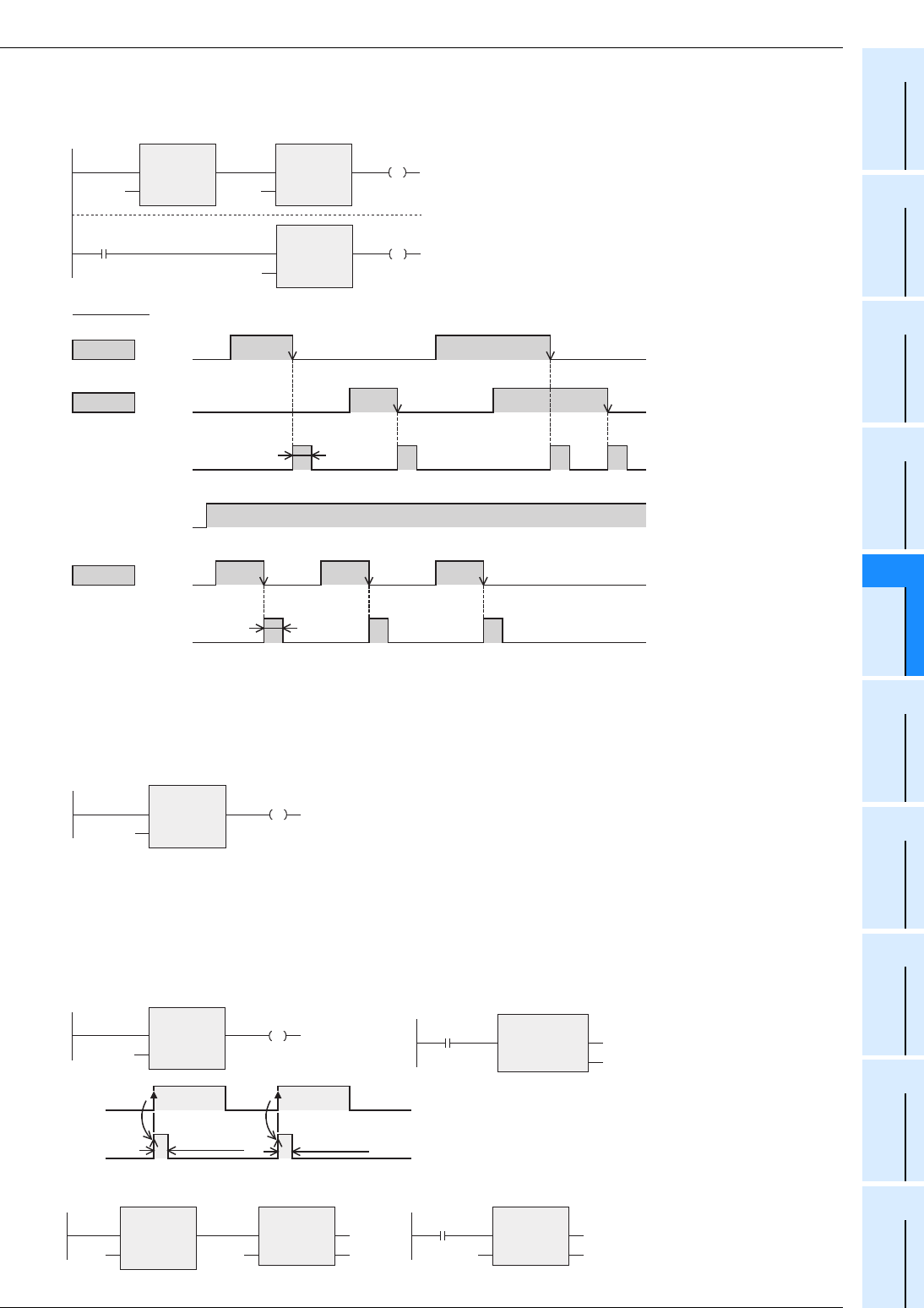
2. LDF, ANDF, ORF (Initial logical operation of falling/trailing edge pulse, serial connection
and parallel connection)
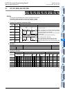
In the example shown above, M0 or M1 is ON during only one operation cycle when X000 to X002 turn OFF
from ON.
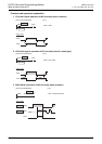
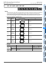
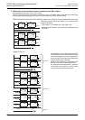
3. Bit specification of data register (D)
A bit data register (D) can be specified as a device used in LDP, LDF, ANDP, ANDF, ORP and ORF
instructions.
When specifying a bit in data register, input "."
after a data register (D) number, and then input
a bit number (0 to F) consecutively.
Only 16-bit data resister is applicable.
Specify a bit number as "0 1, 2, ..., 9, A, B, ..., F"
from the least significant bit.
Example: In the example shown on the left, LDP
contact turns ON (becomes
conductive) or OFF (becomes
nonconductive) when the bit 3 of D0
turns ON or OFF.
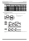
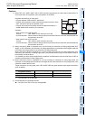
4. Output drive side
The following two circuits offer the same operation.
In each circuit, M6 is ON during only one operation cycle when X010 turns ON from OFF.
In each circuit, MOV instruction is executed only once when X020 turns ON from OFF.
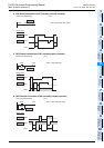
M0:=ORF(LDF(TRUE,X000),X001);
M1:= ANDF(M8000,X002);
[Structured ladder/FBD] [ ST ]
M8000
ANDF
EN
s
ENO
X002
M1
X000
LDF
EN
s
ENO
M0
ORF
EN
s
ENO
X001
RUN monitor
ON
ON ON
ON
timing chart
ORF
LDF
X000
M0
X001
ON
ON
during one
operation
cycle
M8000
ANDF
M1
X002
ON ON ON
ON
during one
operation
cycle
[Structured ladder/FBD] [ ST ]
Y000:= LDP(TRUE,D0.3);
D0.3
LDP
EN
s
ENO
Y000
=
<OUT instruction> <Pulse instruction>
X010
LDP
EN
s
ENO
M6
One
operation cycle
X010
M 6
One
operation cycle
PLS
EN ENO
d
M6
X010
=
<Rising edge detection> <Pulse instruction (applied instruction)>
MOVP
EN
s
ENO
d
D0K10
X020
X020
LDP
EN
s
ENO
K10
MOV
EN
s
ENO
d
D0