


5 Basic Instruction
5.3 OUT (Excluding timers and counters)
63
FXCPU Structured Programming Manual
[Basic & Applied Instruction]
1
Outline
2
Instruction List
3
Configuration of
Instruction
4
How to Read
Explanation of
Instructions
5
Basic Instruction
6
Step Ladder
Instructions
7
Applied Instructions
(Program Flow)
8
Applied Instructions
(Move and
Compare)
9
Applied Instructions
(Arithmetic and
Logical Operation)
10
Applied Instructions
(Rotation and
Shift Operation)
Function and operation explanation
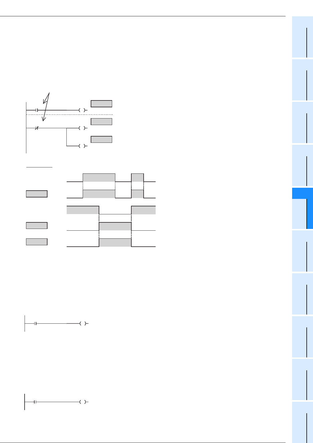
1. When a bit device is used
A device described in OUT instruction turns ON or OFF according to the driven contact status.
Parallel OUT instructions can be used consecutively as many times as necessary.
In the program example shown below, OUT M100 and OUT M101 are parallel.
If two or more OUT instructions are executed for a same device number, however, the double output (double
coil) operation is resulted.
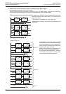
2. Indexing
Devices used in OUT instruction can be indexed with index registers (V and Z).
(State relays (S), special auxiliary relays (M), or "D
.b" cannot be indexed.)
Applicable only to the FX
3U and FX3UC PLCs.
When a used devices is an input (X) or
output (Y), the value of an index register (V
or Z) is converted into an octal number, and
then added.
Example: When the value of Z0 is "20",
Y024 turns ON or OFF.
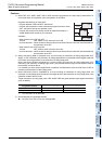
3. Bit specification of data register (D)
A bit in data register (D) can be specified as a device used in OUT instruction.
Applicable only to the FX
3U and FX3UC PLCs.
When specifying a bit in data register, input
"." after a data register (D) number, and then
input a bit number (0 to F) consecutively.
Only 16-bit data resister is applicable.
Specify a bit number as "0 1, 2, ..., 9, A, B,
..., F" from the least significant bit.
Example: In the example shown on the left,
the bit 3 of D0 turns ON or OFF
when X000 turns ON or OFF.
ON
ON
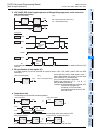
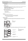
[Structured ladder/FBD] [ ST ]
OUT(X000,Y000);
OUT(NOT X001,M100);
OUT(NOT X001,M101);
For assignment statement
Y000:= X000;
M100:= NOT X001;
M101:= NOT X001;
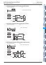
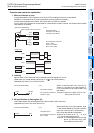
X000
X001
OUT
OUT
OUT
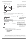
timing chart
OUT
OUT
ONON
X000
ON
Y000
ON
X001
ON
M100
ON
M101
OUT
Drive contact of OUT instruction
Y000
M100
M101
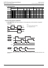
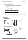
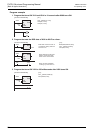
[Structured ladder/FBD] [ ST ]
OUT(X000,Y000Z0);
For assignment statement
Y000Z0:= X000;
X000
Y000Z0
X000
[Structured ladder/FBD] [ ST ]
D0.3
OUT(X000,D0.3);
For assignment statement
D0.3:= X000;