


20
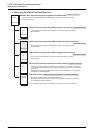
1 Outline
1.2 PLC Series and Programming Software Version
FXCPU Structured Programming Manual
[Basic & Applied Instruction]
1.2 PLC Series and Programming Software Version
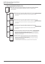
1.3 Cautions on Creation of Fundamental Programs
This section explains cautions on programming.
Refer to the following manual for cautions on structured programs and programming languages:
→ Q/L/F Structured Programming Manual (Fundamentals)
Refer to the following programming manual for detailed operations of and cautions on devices and
parameters:
→ FX Structured Programming Manual [Device & Common]
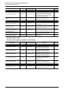
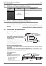
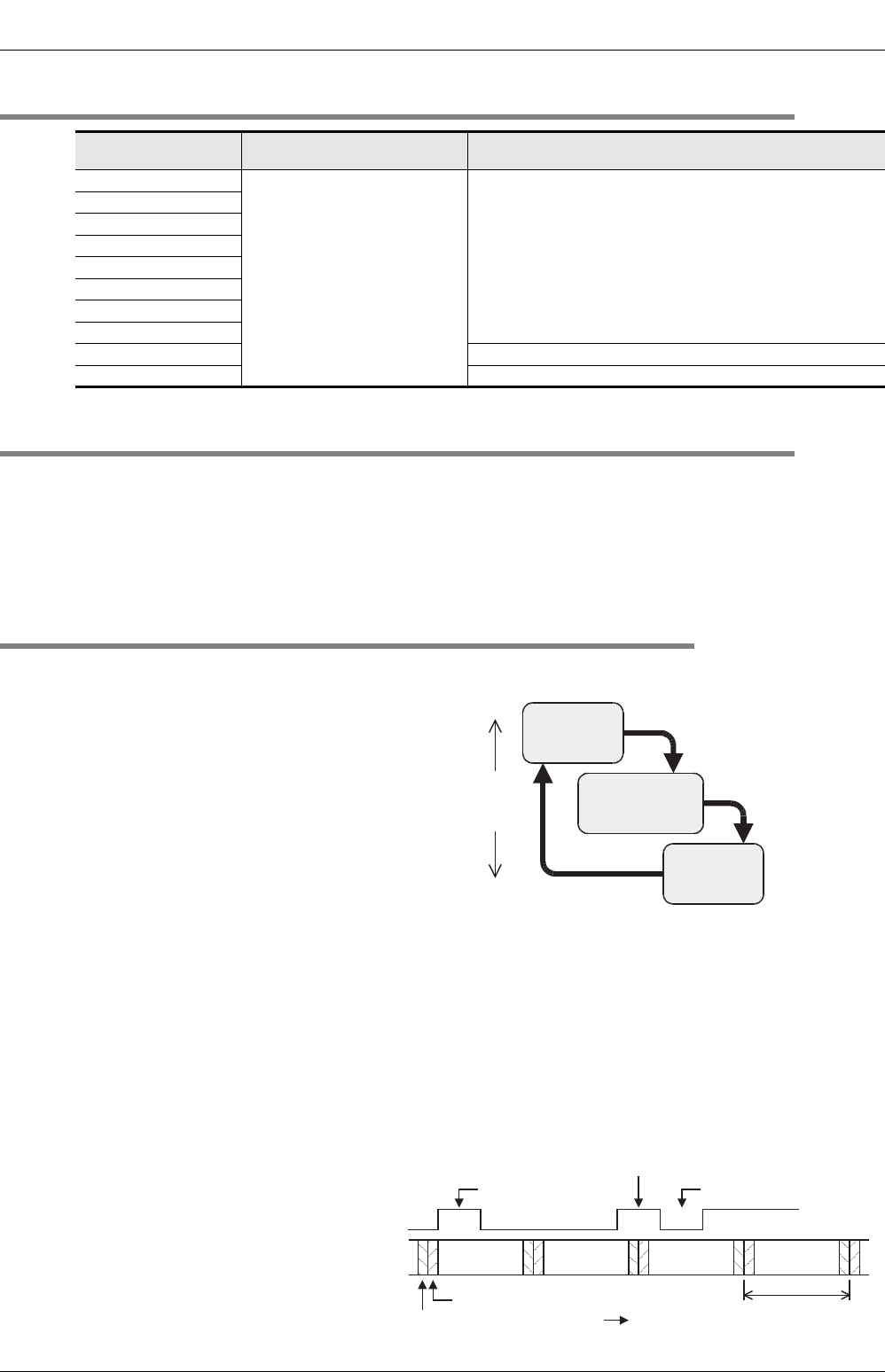
1.3.1 I/O PROCESSING AND RESPONSE DELAY
1. Operation timing of I/O relays and resonse
delay
FX PLCs execute the I/O processing by repeating
the processing (1) to processing (3).
Accordingly, the control executed by PLCs
contains not only the drive time of input filters and
output devices but also the response delay caused
by the operation cycle.
Acquiring the latest I/O information
For acquiring the latest input information or
immediately outputting the operation result in the
middle of the operation cycle shown above, the I/O
refresh instruction "REF" is available.
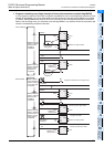
2. Short input pulses cannot be received.
The ON duration and OFF duration of inputs in PLCs require longer time than "PLC scan time + Input filter
response delay."
When the response delay "10 ms" of the input filter is considered and the scan time is supposed as "10 ms",
the ON duration and OFF duration should be at least 20 ms respectively.
Accordingly, PLCs cannot handle input pulses at 25 Hz (1000 / (20+20) = 25) or more. However, the situation
can be improved by PLC special functions and instructions.
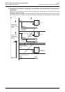
Convenient functions for
improvement
By using the following functions, PLCs
can receive pulses shorter than the
operation cycle.
• High speed counter function
• Input interrupt function
• Pulse catch function
• Input filter value adjustment function
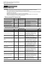
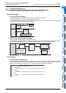
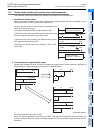
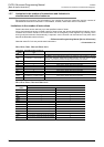
PLC series
Software package name
(model name)
GX Works2 version
FX3U•FX3UC
GX Works2
(SW1DNC-GXW2-E)
Ver. 1.08J or later
FX3G
FX2N•FX2NC
FX1N•FX1NC
FX1S
FXU•FX2C
FX0N
FX0•FX0S
FX3GC Ver. 1.77F or later
FX3S Ver. 1.492N or later
[Input processing]
Input image
memory is read.
[Output processing]
Result is transferred
to output latch
memory.
The ON/OFF status of input terminals
is received at one time.
Input image is read,
and operation is
executed according
to program.
Output
devices
are driven.
Batch I/O method
(refresh method)
(1)
(3)
Scan
time
(operation
cycle)
[Program processing]
Image memory of
each device is updated.
(2)
Program
processing
Program
processing
Program
processing
Program
processing
ON ON
OFFOFF
This "input ON"
cannot be received.
This "input ON" can be received.
This "input OFF"
cannot be received.
Input processing
( Time)
Output
processing
Operation cycle