


847
FX3G/FX3U/FX3UC Series Programmable Controllers
Programming Manual - Basic & Applied Instruction Edition
37 Operation of Special Devices (M8000 -, D8000 -)
37.1 Special Device List (M8000 -, D8000 -)
31
FNC275-FNC279
Data
Transfer 3
32
FNC280-FNC289
High Speed
Processing 2
33
FNC290-FNC299
Extension File
Register
34
FNC300-FNC305
FX
3U
-CF-ADP
35
SFC•STL
Programming
36
Interrupt
Function
37
Special Device
38
Error Code
A
Version Up
Information
B
Execution Times
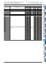
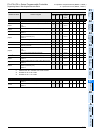
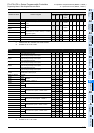
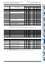
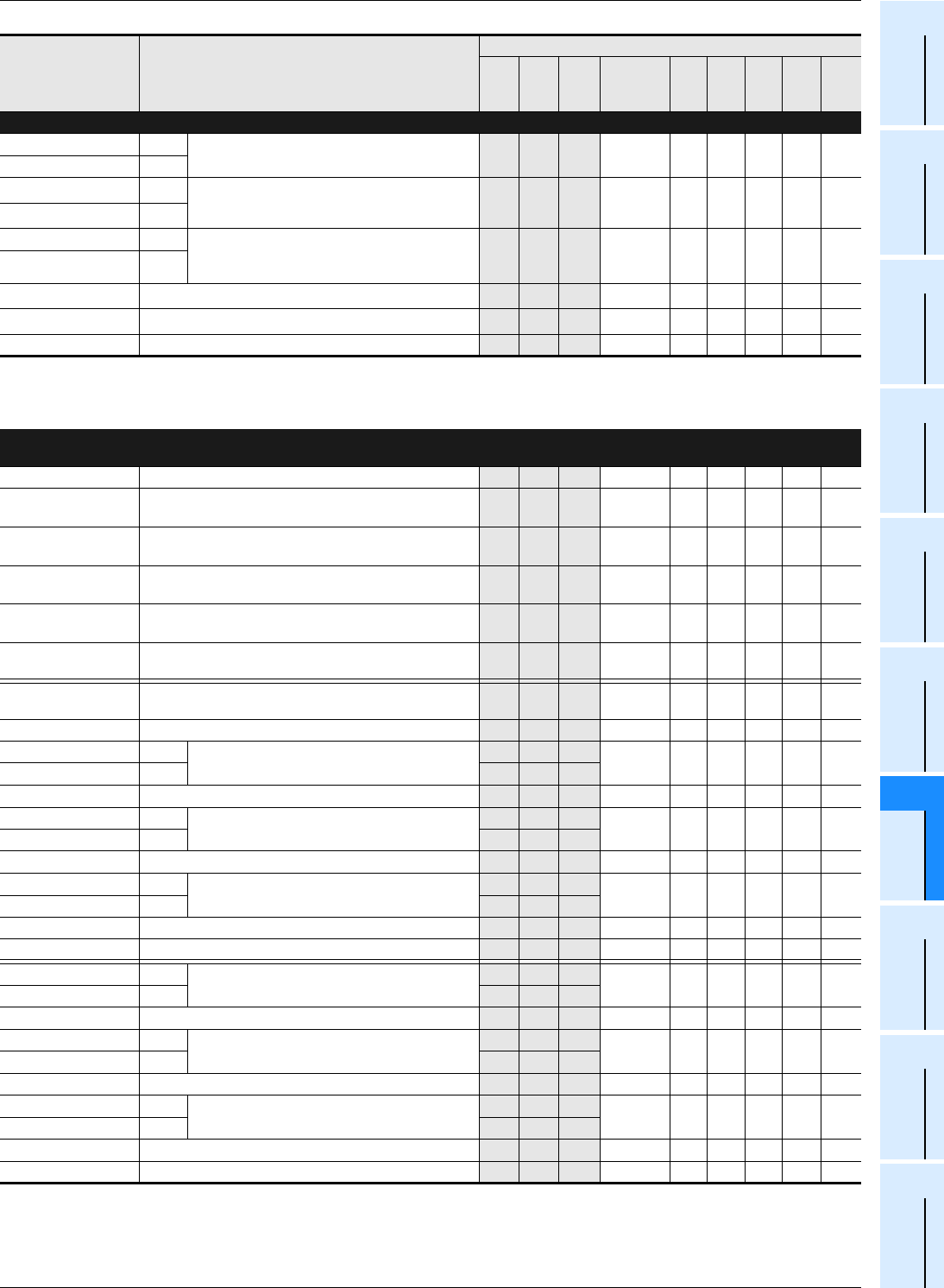
Syntax, Circuit, Operation, or Unconnected I/O Designation Error Step Number (Refer to Chapter 38 for details.)
D 8312 Lower
Operation error step number latched
(32-bit)
– 3 3 M8068–––– –
D 8313 Upper
[D]8314
*1
Lower
Error step number of M8065 to M8067
(32-bit)
– 3 3
M8065 to
M8067
–––– –
[D]8315
*1
Upper
[D]8316 Lower Step number of instruction specifying an
unconnected I/O number (directly or indirectly
using index register)
– 3 3 M8316–––– –
[D]8317 Upper
[D]8318 BFM initialization function: Error unit number
– 3
3
*2
M8318–––––
[D]8319 BFM initialization function: Error BFM number
– 3
3
*2
M8318–––––
[D]8320 to [D]8328 Not used
– – – – –––– –
*1. Cleared when PLC switches from STOP to RUN.
*2. Available in Ver. 2.20 or later.
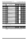
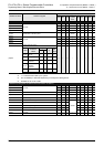
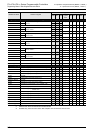
Timing Clock (Refer to Section 24.3 for details.) and Positioning [FX
3G
, FX
3U
and FX
3UC
PLCs] (Refer to Positioning Control Edition for
details.)
[D]8329 Not used – – – – –––– –
[D]8330
DUTY (FNC186) instruction:
Scan counting for timing clock output 1
– 3
3
*3
– –––––
[D]8331
DUTY (FNC186) instruction:
Scan counting for timing clock output 2
– 3
3
*3
– –––––
[D]8332
DUTY (FNC186) instruction:
Scan counting for timing clock output 3
– 3
3
*3
– –––––
[D]8333
DUTY (FNC186) instruction:
Scan counting for timing clock output 4
– 3
3
*3
– –––––
[D]8334
DUTY (FNC186) instruction:
Scan counting for timing clock output 5
– 3
3
*3
– –––––
D 8336
DVIT (FNC151) instruction:
Specification of interrupt input
– 3
3
*4
M8336–––––
[D]8337 to [D]8339 Not used
– – – – –––– –
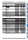
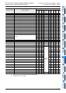
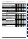
D 8340 Lower
[Y000] Current value register
Default: 0
3 3 3
– –––––
D 8341 Upper
3 3 3
D 8342 [Y000] Bias speed Default: 0
3 3 3 – –––––
D 8343 Lower
[Y000] Maximum speed Default: 100000
3 3 3
– –––––
D 8344 Upper
3 3 3
D 8345 [Y000] Creep speed Default: 1000
3 3 3 – –––––
D 8346 Lower
[Y000] Zero return speed Default: 50000
3 3 3
– –––––
D 8347 Upper
3 3 3
D 8348 [Y000] Acceleration time Default: 100
3 3 3 – –––––
D 8349 [Y000] Deceleration time Default: 100
3 3 3 – –––––
D 8350
Lower
[Y001] Current value register Default: 0
3 3 3
– –––––
D 8351 Upper
3 3 3
D 8352 [Y001] Bias speed Default: 0
3 3 3 – –––––
D 8353 Lower
[Y001] Maximum speed Default: 100000
3 3 3
– –––––
D 8354 Upper
3 3 3
D 8355 [Y001] Creep speed Default: 1000
3 3 3 – –––––
D 8356 Lower
[Y001] Zero return speed Default: 50000
3 3 3
– –––––
D 8357 Upper
3 3 3
D 8358 [Y001] Acceleration time Default: 100
3 3 3 – –––––
D 8359 [Y001] Deceleration time Default: 100
3 3 3 – –––––
*3. Available in Ver. 2.20 or later.
*4. Available in Ver. 1.30 or later.
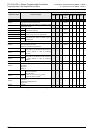
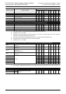
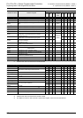
Number and name Content of register
Applicable model
FX
3G
FX
3U
FX
3UC
Correspond-
ing special
device
FX
1S
FX
1N
FX
2N
FX
1NC
FX
2NC