


191
FX3G/FX3U/FX3UC Series Programmable Controllers
Programming Manual - Basic & Applied Instruction Edition
7 Basic Instruction
7.5 LDP, LDF, ANDP, ANDF, ORP, ORF
1
Introduction
2
Overview
3
Instruction
List
4
Devices
in Detail
5
Specified the
Device &
Constant
6
Before
Programming
7
Basic
Instruction
8
FNC00-FNC09
Program Flow
9
FNC10-FNC19
Move & Compare
10
FNC20-FNC29
Arith. & Logic
Operation
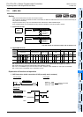
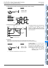
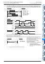
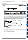
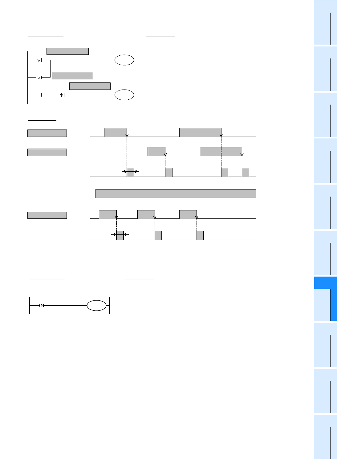
2. LDF, ANDF, and ORF instructions (initial logical operation of falling/trailing edge pulse, serial
connection of falling/trailing edge pulse, and parallel connection of falling/trailing edge pulse)
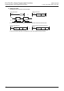
In the example shown above, M0 or M1 is ON during only one operation cycle when X000 to X002 turn OFF from ON.
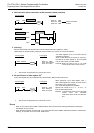
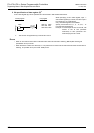
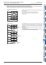
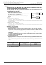
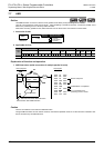
3. Bit specification of a data register (D)
*1
A bit in data register (D) can be specified as a device used in LDP, LDF, ANDP, ANDF, ORP and ORF instructions.
When specifying a bit in data register, input "."
after a data register (D) number, and then input a
bit number (0 to F) consecutively.
Only 16-bit data registers are available.
Specify a bit number as "0, 1, 2, ... 9, A, B, ... F"
from the least significant bit.
Example: In the example shown on the left, LDP
contact turns ON (becomes
conductive) or OFF (becomes non-
conductive) when the bit 3 of D0 turns
ON or OFF.
*1. This function is supported only in FX
3U
/FX3UC PLCs.
X000
X001
M0
M8000 X002
M1
RUN monitor
0000
LDF
X000
0002
ORF
X001
0004 OUT M0
0005 LD M8000
0006
ANDF
X002
0008 OUT M1
ON
ON ON
ON
Timing chart
ORF instruction
LDF instruction
X000
M0
X001
ON
ON during
one opera-
tion cycle
M8000
ANDF instruction
M1
X002
ON ON ON
ON during
one opera-
tion cycle
Circuit program List program
LDF instruction
ORF instruction
ANDF instruction
D0.3
Y000
Circuit program List program
LDP
OUT
0000
0003
D0.3
Y000