


181
FX3G/FX3U/FX3UC Series Programmable Controllers
Programming Manual - Basic & Applied Instruction Edition
7 Basic Instruction
7.2 OUT
1
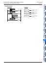
Introduction
2
Overview
3
Instruction
List
4
Devices
in Detail
5
Specified the
Device &
Constant
6
Before
Programming
7
Basic
Instruction
8
FNC00-FNC09
Program Flow
9
FNC10-FNC19
Move & Compare
10
FNC20-FNC29
Arith. & Logic
Operation
2. When a timer or counter is used
The set value is required after OUT instruction for the counting coil of a timer or counter.
The set value can be specified directly by a decimal number (K) or indirectly using a data register (D) or extension
register (R).
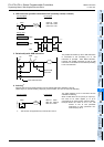
1) Direct specification
The set value of a timer or counter can be
specified directly by a decimal number (K).
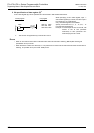
2) Indirect specification
The set value of a timer or counter can be set
by a data register (D) or extension data
register (R). At this time, the current value of
the data register (D) or extension register (R)
is regarded as the set value of the timer or
counter.
It is necessary to write in advance the set
value to a data register (D) or extension
register (R) used for the set value by MOV
instruction, DSW instruction or display unit
before driving the timer or counter.
3) Setting range of timers and counters
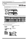
The table below shows the set value range of timers and counters, the actual timer constants and the number of
program steps (including the set value) for OUT instruction.
Timer/counter
Setting range
(Value of K or current value of D or R)
Actual set value Number of steps
1 ms timer 1 to 32767 0.001 to 32.767 sec 3
10 ms timer
1 to 32767
0.01 to 327.67 sec
3
100 ms timer 0.1 to 3276.7 sec
16-bit counter 1 to 32767 Same as left 3
32-bit counter −2,147,483,648 to +2,147,483,647 Same as left 5
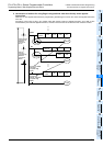
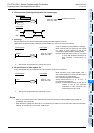
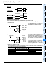
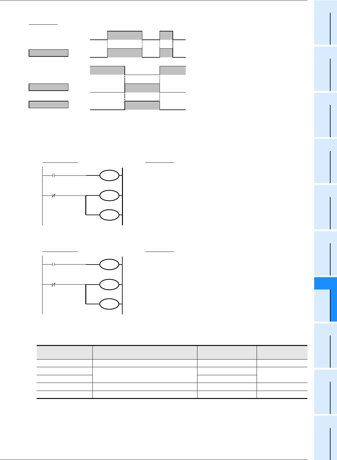
ON
ON
Timing chart
OUT instruction
OUT instruction
ONON
X000
ON
Y000
ON
X001
ON
M100
ON
M101
OUT instruction
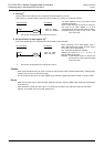
X000
X001
T1
C0
K50
T0
K30
K30
Circuit program
List program
LD
OUT
(SP)
LDI
OUT
(SP)
OUT
(SP)
0000
0001
0004
0005
0008
X000
T0
K30
X001
T1
K30
C0
K50
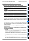
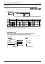
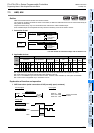
X000
X001
T11
C10
D20
T10
D10
R15
Circuit program
List program
LD
OUT
(SP)
LDI
OUT
(SP)
OUT
(SP)
0000
0001
0004
0005
0008
X000
T10
D10
X001
T11
R15
C10
D20