


3 - 19
MELSEC-Q
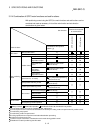
3 SPECIFICATIONS AND FUNCTIONS
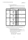
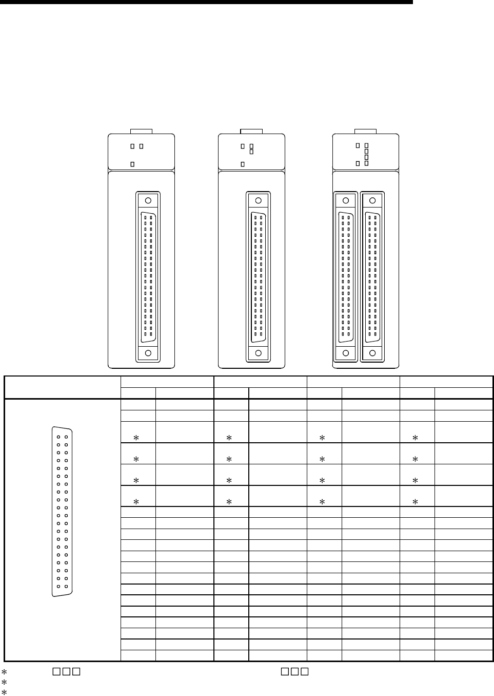
3.4.2 Signal layout for external device connection connector
The specifications of the connector section, which is the input/output interface for the
QD75 and external device, are shown below.
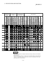
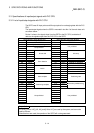
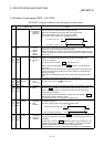
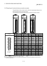
The signal layout for the QD75 external device connection connector is shown.
QD75P1
RUN
ERR
AX1
AX1
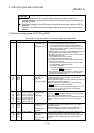
QD75P2
RUN
ERR
AX1
AX1
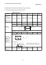
QD75P4
RUN
ERR
AX1
AX1
AX2
AX2
AX2
AX3
AX4
AX2
AX3
AX4
Axis 4(AX4) Axis 3(AX3) Axis 2(AX2) Axis 1(AX1)
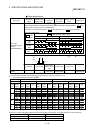
Pin layout
Pin No. Signal name Pin No. Signal name Pin No. Signal name Pin No. Signal name
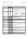
2B20 Vacant 2A20 Vacant 1B20 PULSER B– 1A20 PULSER B+
2B19 Vacant 2A19 Vacant 1B19 PULSER A– 1A19 PULSER A+
2B18
3
PULSE COM
PULSE R–
2A18
3
PULSE COM
PULSE R–
1B18
3
PULSE COM
PULSE R–
1A18
3
PULSE COM
PULSE R–
2B17
3
PULSE R
PULSE R+
2A17
3
PULSE R
PULSE R+
1B17
3
PULSE R
PULSE R+
1A17
3
PULSE R
PULSE R+
2B16
3
PULSE COM
PULSE F–
2A16
3
PULSE COM
PULSE F–
1B16
3
PULSE COM
PULSE F–
1A16
3
PULSE COM
PULSE F–
2B15
3
PULSE F
PULSE F+
2A15
3
PULSE F
PULSE F+
1B15
3
PULSE F
PULSE F+
1A15
3
PULSE F
PULSE F+
2B14 CLRCOM 2A14 CLRCOM 1B14 CLRCOM 1A14 CLRCOM
2B13 CLEAR 2A13 CLEAR 1B13 CLEAR 1A13 CLEAR
2B12 RDYCOM 2A12 RDYCOM 1B12 RDYCOM 1A12 RDYCOM
2B11 READY 2A11 READY 1B11 READY 1A11 READY
2B10 PGOCOM 2A10 PGOCOM 1B10 PGOCOM 1A10 PGOCOM
2B9 PG05 2A9 PG05 1B9 PG05 1A9 PG05
2B8 PG024 2A8 PG024 1B8 PG024 1A8 PG024
2B7 COM 2A7 COM 1B7 COM 1A7 COM
2B6 COM 2A6 COM 1B6 COM 1A6 COM
2B5 CHG 2A5 CHG 1B5 CHG 1A5 CHG
2B4 STOP 2A4 STOP 1B4 STOP 1A4 STOP
2B3 DOG 2A3 DOG 1B3 DOG 1A3 DOG
2B2 RLS 2A2 RLS 1B2 RLS 1A2 RLS
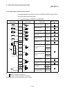
A1
A2
A3
A4
A5
A6
A7
A8
A9
A10
A11
A12
A13
A14
A15
A16
A17
A18
A19
A20
B1
B2
B3
B4
B5
B6
B7
B8
B9
B10
B11
B12
B13
B14
B15
B16
B17
B18
B19
B20
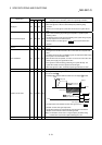
Front view of
the module
2B1 FLS 2A1 FLS 1B1 FLS 1A1 FLS
1: Pin No. "1
" indicates the pin No. for the right connector. Pin No. "2
" indicates the pin No. for the left connector.
2: When a 1-axis module is used, pin Nos. 1B1 to 1B18 are "vacant".
3: The upper line indicates the signal name for the QD75P1/QD75P2/QD75P4, and the lower line indicates the signal name for the
QD75D1/QD75D2/QD75D4.