


QPC513 Enhanced Serial Data Interface card Page 847 of 894
Circuit Card Description and Installation
Connector pin assignments
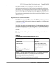
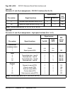
Table 263 shows the pin assignments for J1 and J2 when the port is
configured for RS-232-C interface, and Table 264 on page 848 shows the pin
assignments for J1 and J2 when the port is configured for the high-speed
interface.
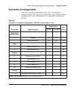
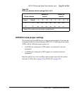
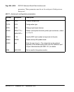
Table 263
Connector J1 and J2 pin assignments – RS-232-C interface (Part 1 of 2)
Pin number Signal functions
Signal source
EIA
circuit
To DCE From DCE
Ground and
common return
1 Shielded n/a n/a
7 Signal ground (SG) n/a n/a AB
Data
2 Transmitted data (TX) 3 — BA
3 Received data (RX) — 3 BB
Control
4 Request to send (RTS) 3 — CA
5 Clear to send (CTS) — 3 CB
6 Data set ready (DSR) — 3 CC
8 Carrier detect (CD) — 3 CF
20 Data terminal ready (DTR) 3 — CD
Timing
15 Transmitter signal element timing (DCE) — 3 DB
Note: Pins not used are 9 to 14, 16, 18, 19, 21, 22, 25.