


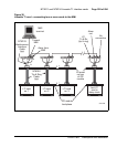

NT5D11 and NT5D14 Lineside T1 Interface cards Page 205 of 894
Circuit Card Description and Installation
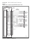
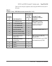
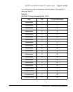
Table 81 shows the pin assignments when using the NT5D13AA lineside T1
I/O cable.
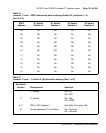
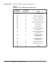
Table 81
Lineside T1 card – NT5D13AA connector pinouts (Part 1 of 2)
I/O panel
connector
pin
Lead designations
NT5D13AA
Lineside
T1 I/O
connector
pin
Lineside T1 cable
connector to external
equipment
1 T1 Tip Receive Data 11 DB15 male to T1 (P2)
Lineside T1 card is CPE
transmit to network and
receive from network
26 T1 Ring Receive Data 3
2 T1 Tip Transmit Data 1
27 T1 Ring Transmit Data 9
3 Alarm out common 1 DB9 male to external alarm (P3)
28 Alarm out (normally open) 2
4 Alarm out (normally closed) 3
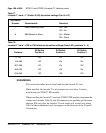
7 Towards MMI terminal
Receive Data
2 DB9 male towards MMI (P5)
Wired as DCE
Data is transmitted on pin 2 (RXD)
and received on pin 3 (TXD)
31 Towards MMI terminal
Transmit Data
3
33 Ground 5
8 Control 1 7
32 Control 2 9