


232 Software Developer’s Manual
Register Descriptions
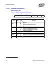
13.4.5 Flash Access
1
FLA (0001Ch; R/W)
This register provides software direct access to the Flash memory. Software can control the Flash
device by successive writes to this register. Data and address information is clocked into the Flash
memory by software toggling the FL_SCK bit (0) of this register with FL_CE set to 1b. Data
output from the Flash memory is latched into bit three of this register via the internal 125 MHz
clock and is accessed by software via reads of this register.
1. Applicable to the 82541xx and 82547GI/EI only.
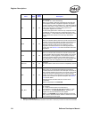
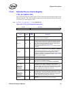
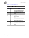
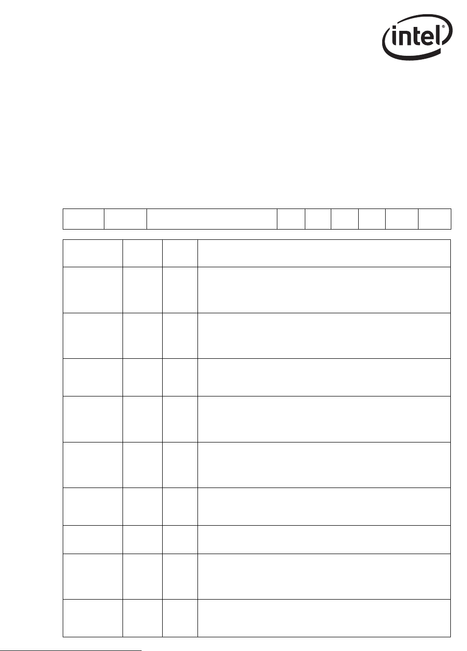
Table 13-9. Flash Access – FLA
31 30 29 - 6 5 4 3 2 1 0
FL
ER
FL
BS
Reserved
FL
GNT
FL
REQ
FL
SO
FL
SI
FL
CS
FL
SCK
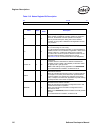
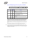
Field Bit(s)
Initial
Value
Description
FL_SCK 0 0b
Clock Input to the FLASH.
When FL_GNT is 1b, the FL_SCK out signal is mapped to this bit and
provides the serial clock input to the Flash device. Software clocks the
Flash memory via toggling this bit with successive writes.
FL_CE 1 0b
Chip FL Input to the FLASH.
When FL_GNT is 1b, the FL_CS output signal is mapped to the chip
select of the device. Software enables the FLASH by writing a 0b to this
bit.
FL_SI 2 0b
Data Input to the FLASH.
When FL_GNT is 1b, the FL_DI output signal is mapped directly to this
bit. Software provides data input to the FLASH via writes to this bit.
FL_SO 3 X
Data Output Bit from the FLASH.
The FL_SO input signal is mapped directly to this bit in the register and
contains the Flash memory serial data output. This bit is read only from
the software perspective — writes to this bit have no effect.
FL_REQ 4 0b
Request FLASH Access.
The software must write a 1b to this bit to get direct Flash memory
access. It has access when FL_GNT is 1b. When the software
completes the access it must write a 0b.
FL_GNT 5 0
Grant FLASH Access.
When this bit is 1b, the software can access the Flash memory using
the FL_SCK, FL_CE, FL_SI, and FL_SO bits.
Reserved 29:6 0
Reserved.
Reads as 0b.
FL_BUSY 30 0
Flash Busy.
This bit is set to 1b while a write or an erase to the Flash memory is in
progress. While this bit is clear (read as 0b) software can access to
write a new byte to the Flash device.
FL_ER 31 0
Flash Erase Command.
This command will be sent to the Flash component only if bits 5:4 are
also set. This bit is automatically cleared and read as 0b.