


Software Developer’s Manual 125
FLASH Memory Interface
FLASH Memory Interface 7
All Ethernet controllers (except the 82540EP/EM) provide an external parallel interface to a
FLASH, or boot ROM, device such as the Atmel AT49LV010
1
. All accesses to this device are
managed by the Ethernet controller and are accessible to software as normal PCI reads or writes to
the FLASH memory mapping range. The Ethernet controller supports parallel FLASH devices
with up to 4 Mb (512 KB) of memory. The size of the FLASH implemented with the Ethernet
controller can be encoded into bits in the EEPROM. The FLASH and Expansion ROM Base
Address Registers are reconfigured based on these EEPROM settings.
Note: Though the Ethernet controller supports devices with up to 512 KB of memory, smaller devices can
also be used. Accesses to memory beyond the FLASH device size results in access wrapping as
only the lower address bits are utilized by the FLASH.
7.1 FLASH Interface Operation
The FLASH is read from, or written to, each time the host processor performs a read or a write
operation to a memory location that is within the FLASH address mapping or upon boot through
accesses in the space indicated by the Expansion ROM Base Address Register (see Section 4.1).
All accesses to the FLASH, except read accesses, require the appropriate command sequence for
the device used. Refer to the specific FLASH data sheet for more details on reading from or writing
to FLASH. Accesses to the FLASH are based on a direct decode of processor accesses to a memory
window defined in either the Ethernet controller's FLASH Base Address Register (PCI Control
Register at offset 14h or 18h) or the Expansion ROM Base Address Register (PCI Control Register
at offset 30h).
FLASH accesses must always be assembled or disassembled by the Ethernet controller to or from
the FLASH whenever the access is greater than a byte-wide access. Due to slow access times to a
typical FLASH, word (32-bit) accesses are not recommended for any cycles that occur after system
initialization in order to avoid violating PCI hold specifications. Boot ROM shadowing is an
exception to the 16 clock rule and can incur in excess of 25 wait states. The Ethernet controller byte
reads to the FLASH take approximately of 256 ns. The Ethernet controller issues retry accesses
during this time.
7.2 FLASH Control and Accesses
Write control of the FLASH is controlled by the FWE bits in the EEPROM/FLASH Control and
Data Register (EECD.FWE). See Section 13.4.3 for details.
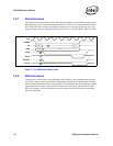
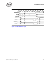
Processor accesses to the FLASH are very slow. The Ethernet controller always issues a target-
disconnect at the first data cycle. The Ethernet controller asserts the STOP# signal to indicate the
target-disconnect. Section 7.2.1 and Figure 7.2.2 show read and write accesses to the FLASH. Note
that burst accesses to the FLASH address space are not allowed.
1. The 82540EP/EM provides an external interface to a serial FLASH or Boot EEPROM device. See Appendix B for more information.