


136 Software Developer’s Manual
Power Management
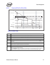
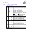
6.3.2.4 PCI Reset Without Transition to D3
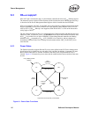
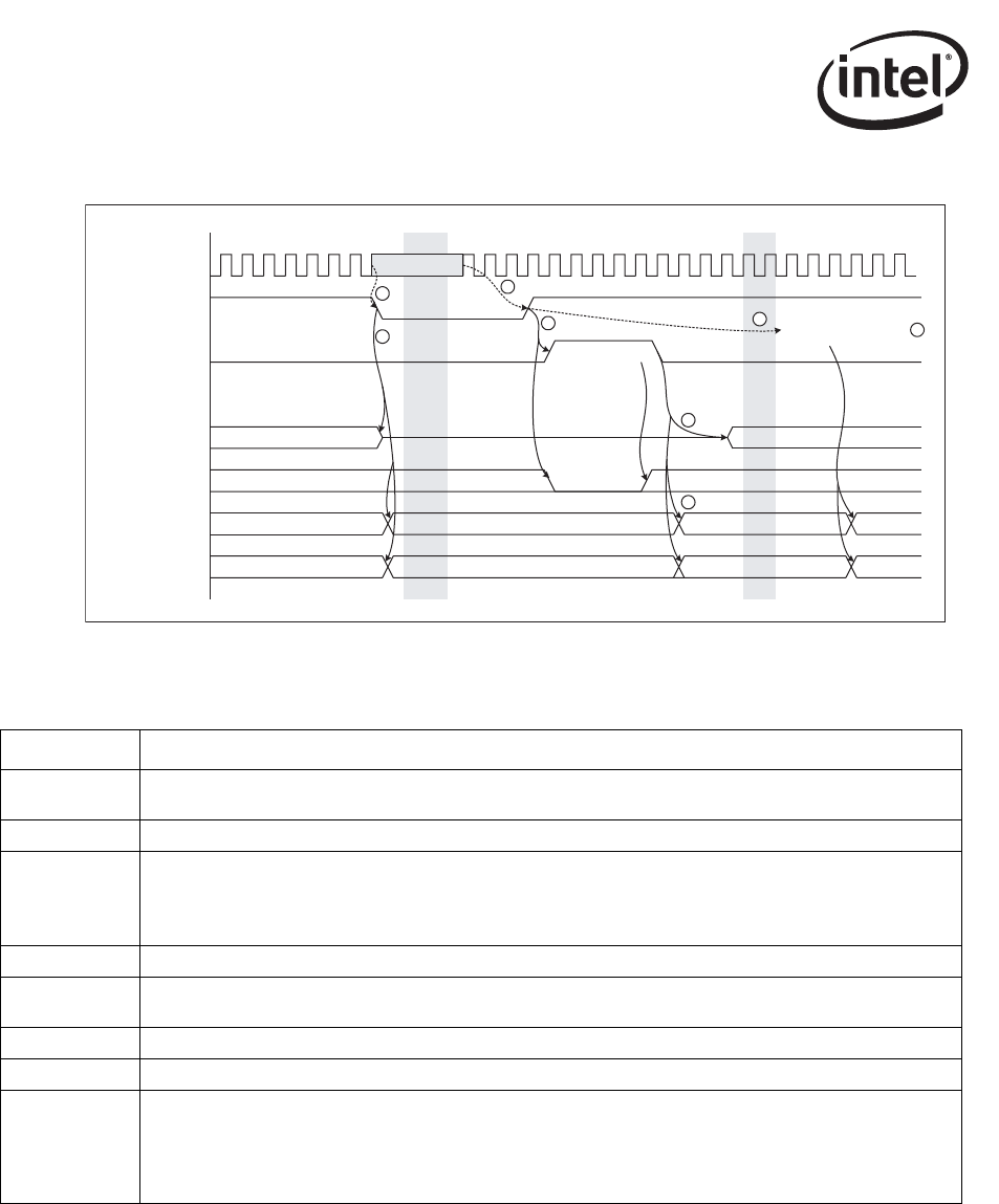
Figure 6-5. PCI Reset Sequence
CLK#
RST#
DState
PWR_STATE[1:0]
D0u
Reading EEPROM
Read EEPROM
D0a
ELIZDNHXSLVGLVDEOHGELIZDNHXSLVHQDEOHG E
MemoryAccess Enable
PCI Pins
Running
Wakeup Enabled
Dr
6
Any mode APM Wakeup
E
D0a
Running
7
1
2
3
4
5
EE
8
*&(,2QO\
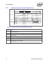
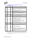
Diagram # Notes
1
In 66 MHz or PCI-X
a
modes, the system must assert RST# before stopping the PCI clock. It may assert RST#
without stopping the clock.
2 Upon assertion of RST# the Ethernet controller floats all PCI pins except PME# and goes to “Dr” state.
3
In 66 MHz or PCI-X modes the system must assert RST# before stopping the PCI clock. It may assert RST#
without stopping the clock.
For the 82541PI/GI/EI and 82540EP, If CLK_RUN# is enabled, then they do not require a continuous clock
during this time, but does require that the system drive the clock in response to CLK_RUN# assertion.
4 The deassertion edge of RST# caused the EEPROM to be re-read and Wakeup disabled.
5
Synchronizing the clock circuits and circuit adjustments require up to 512 PCI clocks before the Ethernet
controller drives PCI signals and responds to PCI transactions.
6 For the 82544GC/EI, PWR_STATE[1:0] is set to 01b if APM Wakeup is enabled, 00b otherwise.
7 The system can delay an arbitrary time before enabling memory access.
8
Writing a 1b to the Memory Access Enable or I/O Access Enable bit in the PCI Command Register transitions
the Ethernet controller from D0u to D0 state.
For the 82544GC/EI, writing a 1b to the Memory Access Enable or I/O Access Enable bit in the PCI
Command Register transitions the Ethernet controller from D0u to D0 state and asserts both PWR_STATE
outputs.
a. Not applicable to the 82541xx, 82547GI/EI, or 82540EP/EM.