


228 Software Developer’s Manual
Register Descriptions
13.4.3 EEPROM/Flash Control & Data Register
EECD (00010h; R/W)
This register provides a simplified interface for software accesses to the EEPROM. Software
controls the EEPROM by successive writes to this register.
Data and address information is clocked into the EEPROM by software toggling the EECD.SK bit
(2) of this register with EECD.CS set to 1b.
Data output from the EEPROM is latched into bit 3 of this register and can be accessed by software
through reads of this register.
See Section 5 for more detailed EEPROM information.
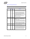
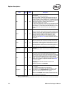
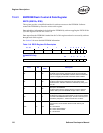
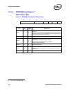
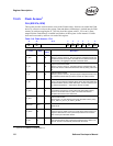
Table 13-6. EECD Register Bit Description
82544GC/EI Only
31 - 10 9 8 7 6 5 4 3 2 1 0
Reserved SIZE PRES GNT REQ FWE
D
O
DI CS SK
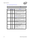
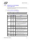
31 65 43210
Reserved FWE DO DI CS SK
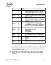
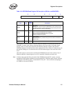
Field Bit
Initial
Value
Description
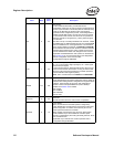
SK 0 0b
Clock input to the EEPROM
The EESK output signal is mapped to this bit and provides the
serial clock input to the EEPROM. Software clocks the EEPROM
by means of toggling this bit with successive writes to EECD.
CS 1 0b
Chip select input to the EEPROM
The EECS output signal is mapped to the chip select of the
EEPROM device. Software enables the EEPROM by writing a 1b
to this bit.
DI 2 0b
Data input to the EEPROM
The EEDI output signal is mapped directly to this bit. Software
provides data input to the EEPROM through writes to this bit.
DO 3 X
Data output bit from the EEPROM
The EEDO input signal is mapped directly to this bit in the register
and contains the EEPROM data output. This bit is read-only from
the software perspective – writes to this bit have no effect.
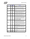
FWE 5:4 01b
Flash Write Enable Control
These two bits, control whether writes to Flash memory are
allowed.
00b = Not allowed
01b = Flash writes disabled
10b = Flash writes enabled
11b = Not allowed