


212 Software Developer’s Manual
Register Descriptions
• Reserved and/or undefined addresses. Any register not explicitly declared in this
specification should be considered to be reserved and should not be written. Writing to
reserved or undefined register addresses can cause indeterminate behavior. Reads from
reserved or undefined configuration register addresses can return indeterminate values unless
read values are explicitly stated for specific addresses.
• Initial values. Most registers define the initial hardware values prior to being programmed. In
some cases, hardware initial values are undefined and are listed as such via the text
“undefined,” “unknown,” or “X.” Some such values might need setting through EEPROM
configuration or software in order for proper operation to occur; this need is dependent on the
function of the bit. Other registers might cite a hardware default that is overridden by a higher
precedence operation. Operations that might supersede hardware defaults can include a valid
EEPORM load, completion of a hardware operation (such as hardware Auto-Negotiation), or
writing of a different register whose value is then reflected in another bit.
For registers that should be accessed as 32-bit double words, partial writes (less than a 32-bit
double word) is ignored. Partial reads return all 32 bits of data regardless of the byte enables.
Partial reads to read-on-clear registers (for example, ICR) can have unexpected results since all 32
bits are actually read regardless of the byte enables. Partial reads should not be performed.
All statistics registers are implemented as 32-bit registers. 64-bit accesses to these registers must
have the upper byte enables deasserted. 32-bit registers with addresses not on a quadword
boundary cannot be accessed through a 64-bit access.
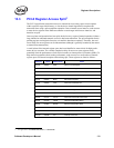
Note: The PHY registers are accessed indirectly through the MDI/O interface.
13.2.1 Memory and I/O Address Decoding
13.2.1.1 Memory-Mapped Access to Internal Registers and Memories
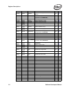
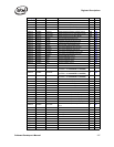
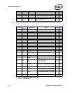
The internal registers and memories can be accessed as direct memory-mapped offsets from the
base address register (BAR0 or BAR0/BAR1, see Section 4.1). Refer to Table 13-2 for the
appropriate offset for each specific internal register.
13.2.1.2 Memory-Mapped Access to FLASH
The external Flash can be accessed using direct memory-mapped offsets from the Flash base
address register (BAR1 or BAR2/BAR3, see Section 4.1). The Flash is only accessible if enabled
through the EEPROM Initialization Control Word, and if the Flash Base Address register contains
a valid (non-zero) base memory address. For accesses, the offset from the Flash BAR corresponds
to the offset into the flash actual physical memory space.
13.2.1.3 Memory-Mapped Access to Expansion ROM
The external Flash can also be accessed as a memory-mapped expansion ROM. Accesses to offsets
starting from the Expansion ROM Base address (see Section 4.1) reference the Flash provided that
access is enabled through the EEPROM Initialization Control Word, and if the Expansion ROM
Base Address register contains a valid (non-zero) base memory address.