


93
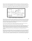
peak load demand. For short term overloads, a quick approximation can be made to determine the amount of
voltage sag:
(I
P
– I
L
) ∆T
∆V≈ =
C
O
where:
∆V = The voltage sag
E
NORM
I
P
=
R
L PEAK
= Peak load current demand,
I
L
= The current limit or constant current setting,
Co = The output capacitor (in farads), and
∆T = Duration of overload condition (in seconds).
This approximation is pessimistic, since it assumes that the discharge of the output capacitor is linear at the rate
of I/C instead of decaying exponentially.
REVERSE CURRENT LOADING
In some applications it is necessary for a power supply to retain its normal regulated output voltage in the
presence of reverse current flow during part of the operating cycle of an active load device connected to the
power supply. Such situations can arise, for example, in pulse and digital circuitry and in bias supplies for class
C amplifiers.
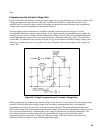
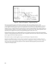
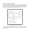
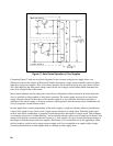
Figure 64A illustrates the nature of this problem. It is assumed that the active load device normally draws a
current of 5 amperes, but that during part of its operating cycle it delivers a current of 3 amperes. Since the
series transistor cannot conduct current in the reverse direction, the reverse current furnished from the load
device would charge the output capacitor of the power supply, causing an increase in the output voltage with
loss of regulation and possible damage to the output capacitor and other components within the power supply.
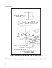
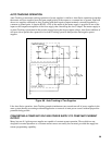
To correct these deficiencies and permit the normal operation of a regulated power supply with loads of this
type, it is only necessary to add a shunt or dummy load resistor such as RD (Figure 64B), thus shifting the zero
bias level with respect to the load current waveform so that the power supply is only required to deliver current.
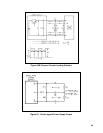
In terms of the numerical example shown in Figure 64B, it is necessary to add a resistor R
D
which will draw 3
(or more) amperes at the operating voltage of the power supply. With this resistor added, the power supply
output current varies between 0 and 8 amperes rather than between -3 and +5 amperes. During the interval
when the load device is absorbing current, current flow follows the paths indicated by the solid lines of Figure
64B, whereas when the load device delivers current, current flow follows the path indicated by the broken line.
Since the power supply is operating normally under both conditions, the voltage across the active load device is
maintained continuously at the regulated level.