


47
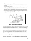
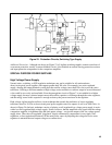
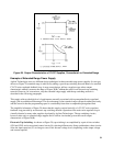
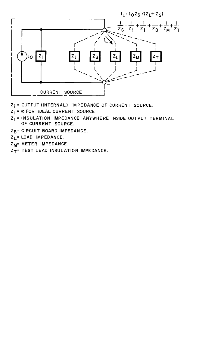
Figure 26. Impedances Shunting the Load Degrade Current Regulation
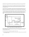
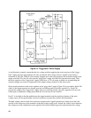
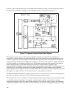
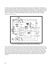
As shown in Figure 27, the CCB design includes three key sections which determine its unique regulating pro-
perties--the Programming/Guard Amplifier, the Main Current Regulator, and the Voltage Limit Circuit.
The Programming/Guard Amplifier is an independent, variable constant voltage source, whose output voltage
E
G
is linearly dependent upon the setting of R
Q
, being equal to E
S
R
Q
/R
S
. The guard aspects of this circuit are
discussed in detail later; it is sufficient to note here that this circuit permits linear output current control while
facilitating the common point connection at the inboard side of the current monitoring resistor.
The Programming/Guard Amplifier provides the programming voltage E
G
for the Main Current Regulator; this
dc voltage, which is negative with respect to circuit common, is applied to one of the inputs of the differential
Current Comparison Amplifier. The other input of this differential amplifier is connected to the current
monitoring resistor R
M
. The Current Comparison Amplifier continuously compares the voltage drop across the
current monitoring resistor (I
O
R
M
) with the programming voltage (E
G
). If these voltages are momentarily
unequal due to a load disturbance or a change in the output current control setting, this error voltage is
amplified and applied to the series regulator transistors, altering the current conducted through them and forcing
the voltage drop I
O
R
M
to once again equal E
G
.
The output current is related to the programming voltage and reference voltage by the relationship
E
G
E
S
R
Q
I
O
=
R
M
=
R
M
•
R
S
As this equation suggests, R
M
is a critical component and is selected to have low noise, low temperature coef-
ficient, and low inductance.