


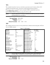


A - Specifications
140
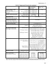
Supplemental Characteristics
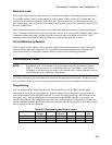
Table A-2 lists the supplemental characteristics, which are not warranted but are descriptions of typical
performance determined either by design or type testing.
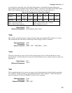
Table A-2. Supplemental Characteristics
Parameter
Agilent 66321B/D;
Agilent 66319B/D
output 1 only
Agilent 66319B/D
output 2 only
Output Programming Range
Voltage:
Current:
Resistance:
Voltage Limit:
0 – 15.535 V
0 – 3.0712 A
– 40 mΩ to 1 Ω
0 – 22 V
0 – 12.25 V
0 – 1.52 A
NA
NA
Average Programming Resolution
Voltage:
Current:
Resistance:
4.2 mV
0.825 mA
1.2 mΩ
14 mV
1.75 mA
NA
Tracking OVP Accuracy
(refer to page 35 for details)
Above programmed
voltage:
2.0V ± 2%
NA
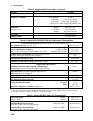
Average Current Measurement
Resolution
3 A Range:
1 A Range:
0.02A Range:
214 µA
32 µA
0.6 µA
55 µA
NA
NA
Maximum Current Measurement
3 A Range:
1 A Range:
0.02A Range:
7 A
1.05 A
21.5 mA
1.8A
NA
NA
Sink Current
- 2 A @ 7.5 V
1
- 0.03 A @ 7.5 V
Programming Accuracy
Temperature Coefficient
(change/C°)
Voltage:
Current:
Resistance:
0.01% + 0.5 mV
0.01% + 15 µA
0.1% + 0.2 mΩ
0.03% + 1.5 mV
0.03% + 0.4 mA
NA
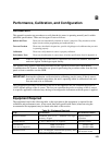
Readback Accuracy Temperature
Coefficient (change/C°)
Voltage:
3 A Current (dc):
3 A Current (acdc):
1 A Current range:
0.02A Current range:
0.01% + 300 µV
0.02% + 15 µA
0.05% + 120 µA
0.01% + 10 µA
0.01% + 0.3 µA
0.02% + 1.5 mV
0.02% + 0.4 mA
NA
NA
NA
Drift
2
Voltage:
Current: +
0.01% + 1 mV
0.01% + 30 µA
0.03% + 3 mV
0.03% + 0.8 mA
Remote Sense Capability
In each load lead up to 4 V
3
up to 4 V
4
Output Voltage Rise Time
Output Voltage Fall Time
10% to 90%:
90% to 10%:
< 200 µs
< 200 µs
< 200 µs
< 35 ms
Output Voltage Settling Time
5
0 to rated voltage:
rated voltage to 0:
0.5 ms
1 ms
NA
NA
Output 2 OFF time
12 V to 2 V: NA
< 200 µs
6
1
The sink current decreases linearly from 2.8A @ 0 V to 1.2 A @ 15 V. Sink current does not track the programmed current.
2
Following a 30 minute warm-up, the change in output over 8 hours, under constant ambient, load and line conditions.
3
Add 2 mV to the load regulation for each 1 V change in the positive output lead.
4
Add 3 mV to the load regulation for each 1 V change in the negative output lead.
5
To settle within 12 mV of the final value for Output 1.
6
When output 2 is turned off or disabled, the output voltage reduces from 12 V to less than 2 V in under 200 µs.