


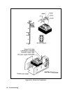
84 Principles Of Operation
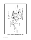
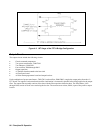
any value of load impedance. Switching between CV and CC is done automatically by the CV/CC control circuits at a
value of load impedance equal to the ratio of the programmed voltage value to the programmed current value.
A low-level CV or CC signal is generated by the applicable status comparator (P/O U502) and returned to the secondary
processor to indicate that the corresponding mode, CV or CC, is in effect.
In CV mode, an OR gate diode (D652) conducts and the CV loop regulates the output voltage. A CV error amplifier (P/O
U621) compares the programmed voltage signal CVPROG to VMON which is the output signal from the V_DIF
amplifier(P/O U621). The range of VMON is 0 volts to +10 volts which corresponds to the zero-to-full-scale output voltage
of the supply. If the output voltage exceeds the programmed voltage the OR GATE signal goes low causing the output
voltage to decrease to the programmed value.
Conversely, if the output voltage is less than the programmed voltage, the OR GATE signal goes high causing the output
voltage to increase to the programmed value. An externally applied dc signal, VPROG, can be used to program the output
voltage. A 0 volt to -5 volt VP level produces a proportional zero-to-full-scale output voltage.
In CC mode, an OR gate diode (D651) conducts and the CC loop regulates the output voltage. A CC error amplifier (P/O
U620) compares the programmed voltage signal CCPROG to IMON which is the output signal of 2nd I_AMP (P/O U620).
The range of IMON is 0 volts to +10 volts which corresponds to the zero-to-full-scale output voltage of the supply. If the
output current exceeds the programmed current, the OR GATE signal goes low causing the output current to decrease to the
programmed value.
Conversely, if the output current is less than the programmed current, the OR GATE signal goes high causing the output
current to increase to the programmed value. An externally applied dc signal, IPROG, can be used to program the output
current. A 0 volt to -5 volt IP level produces a proportional zero-to-full-scale output current.
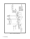
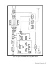
Switching/Downprogramming Control (P/O A10) These circuits include a Ramp Generator, Divider /Deadtime Latch, Fast
Sense Differential Amplifier, Pulse Width Modulator, Summing Comparator, Down-Programmer Control and OV
Comparator circuits.
The Divider/Deadtime Latch (U600, U601, U602) divides the 2-MHz ALE_CK signal from the Secondary µP and supplies
40 KHz pulses to the Ramp Generator (U607) and ON Latch ( U604).
The OR-GATE signal (CV or CC control signal as previously described) is summed with the 40 KHz triangular waveform
produced by the Ramp Generator. An input from the Fast Sense Differential Amplifier is also summed to compensate for a
sudden transient in the rectified output.
The width of the output pulses from the Summing Amplifier vary as the OR-GATE control signal increases or decreases.
These pulses are applied to the Pulse-Width Modulator (U603) via the On Latch. The PWM generates the square wave
pulses that are applied to the A3 FET assembly to turn the FET switches on and off. The Deadtime Latch resets the ON
Latch to provide a minimum off time for the FET switches.
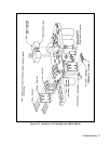
The OV circuit compares the output voltage level with the OVREF signal which represents the programmed overvoltage
level. When the output voltage exceeds the programmed OV value, the downprogrammer circuits are activated and the FET
switches are turned off
The Downprogrammer control circuit generates control signal DP CONTROL whenever an OV or disable condition has
been detected, or when the output voltage exceeds the programmed value. DP CONTROL causes the downprogrammer
FETs (Q980, Q981) on the A9 Downprogrammer/Fast Sense board to conduct and conduct current away from the load.