


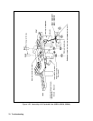

82 Principles Of Operation
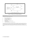
A digital control interface on the A2 GPIB Board provides the following power supply functions:
• Relay link.
• Digital 1/0.
• Remote inhibit (INH).
• Discrete fault indicator (FLT).
An optical isolator IC (U113) isolates the FLT output signal common from the external fault circuit common. The desired
digital interface function is selected by placing a jumper in a header (J106) on the A2 GPIB Board. Appendix D in the
Power Supply Operating Manual describes how to select one of these functions and how to make the appropriate external
connections to the DIG CNTL connector on the supply's rear panel. Another jumper position on the header selects the SA
(signature analysis) mode, which is used for troubleshooting (see Chapter 3).
The A2 Board has a bias supply regulator IC (U121) that provides +5V (with respect to earth ground) for the primary
interface circuits and the bias voltage for the front panel board circuits, the LCD, and the keypad. The A2 Board also has a
line or bias voltage detector IC (U101) that generates a power clear signal (PCLR). This signal initializes certain primary
interface and front panel circuits when normal ac line voltage is applied, and also shuts these circuits down when the line
voltage drops below the required minimum.
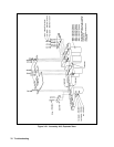
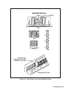
A1 Front Panel Assembly
The power supply A1 Front Panel Assembly contains a circuit board, keypad, liquid crystal display (LCD), and the power
on/off switch.
The Front Panel Circuit Board A1 contains microprocessor circuits (microprocessor U3 and ROM U4) that decode and
execute all front panel keypad commands. These are transferred to the power supply output via the serial I/O port to the A2
board GAL (gated-array logic) IC and isolators, and to the secondary interface circuits on the A10 Control Board. The front
panel microprocessor circuits also process power supply measurement and status data received from the serial I/O port.
This data is displayed on the LCD.
IC EEPROM, U6, (electrically-erasable, programmable, read-only memory) on the A1 Front Panel Board stores data and
configuration information. This information includes calibration constants, GPIB address, the present programming
language, and model-dependent data such as the minimum and maximum values of voltage and current.
One of the EEPROM storage locations holds a checksum value used to verify the integrity of this EEPROM data. Access to
the calibration data in the EEPROM is controlled by the combination of a password and jumper options on a header (J3)
located on the A1 board (see Post-Repair Calibration in Chapter 3).
The power supply can be calibrated manually using the front panel keys, or via the GPIB bus with SCPI (Standard
Commands for Programmable Instruments) commands. The calibration procedure is in Appendix A of the Power Supply
Operating Manual).
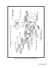
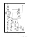
A10 Control Board
The A10 Control Board contains the Secondary Interface, CV/CC Control Circuits, Readback Circuits, PWM Switching
Circuits and OV/Downprogramming Circuits. These circuits are shown schematically in the A10 Control Board schematic.
Secondary Interface (P/O A10 Board)
These circuits are shown in detail on the A10 Control Board schematic and include the Secondary Microprocessor (U506),
Programmed GAL (U505), three DAC/OpAmp circuits (U510-U515), Readback Comparator circuits (U516, U517) and
OV/Shunt DAC OpAmp circuit, (U520, U521).