


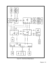
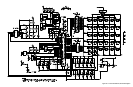
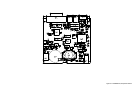
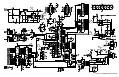

Diagrams 119
Table 6-3. Test Points (continued)
TEST POINT No. & Loc. Signal Tested Measurement and Conditions
A10 Control Board (continued)
U600-10
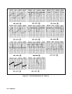
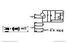
DIVIDER CLOCK (Sheet 3) See Figure 6-1
U601-6
DIVIDER RESET (Sheet 3) See Figure 6-1
U601-3
ON LATCH CLOCK (Sheet 3) See Figure 6-1
U604-3
ON LATCH (Sheet 3) See Figure 6-1
U603-3
PWM_EN (Sheet 3) Held high for approximately 12 seconds at
power-on, then goes low.
U603-13
VOS (Sheet 3)
+5 ± 0.2V
NOTE: Temporarily move both scope leads to J511 for TP
J511-1,2
DRV A, DRV B (Sheet 3) See Figure 6-1
U502-14
+5V
U501-7
OVREF (Sheets 1,3) +5.4V
Q602,C
DP CONTROL (Sheet 3)
CV Mode CC Mode
Not Applicable -0.14V
U608-7
DP CONTROL (Sheet 3) CV Mode CC Mode
+13V 0V
U630-11
PREF_2 (Sheets 1,3) +1V
U630-12
DN PGM (Sheets 1,3) 0V
D660-AN
DP_TST (Sheet 3) 0V
U502-12
OV COMPARATOR (Sheet 3) CV Mode CC Mode
+1.5V +3.25V
General Schematic Notes
The following table lists summary information about notes appearing in schematic diagrams.
Table 6-4. General Schematic Notes
1. All resistors are in ohms ±1%, 1/8W, unless otherwise specified.
2. All capacitors are in microfarads unless otherwise specified.
3. Signal lines that are terminated by flags continue on other sheets, and may also go to other locations on the same sheet.
Example: CVPROG (SH.2 8C); "SH.2 8C" indicates the sheet number and the coordinates on that sheet where the
CVPROG signal line goes.
4. Unterminated signal lines go to a least one other location on the same sheet.
5. Unless otherwise noted, bias connections to integrated-circuit packages are as follows:
Common + 5V
14-pin packages pin 7 pin 14
16-pin packages pin 8 pin 16
20-pin packages pin 10 pin 20