


Operation Overview 25
The rear-panel TRIGGER connector also provides a trigger output signal. This signal is generated synchronously with the
trigger signal sent by the mainframe to the modules. The trigger output signal can be used to trigger an external device such
as an oscilloscope, DVM, or another Electronic Load mainframe.
The Electronic Load has a status reporting capability to keep track of trigger operations. Refer to ’Status Reporting’ in the
Agilent Electronic Loads Programming Reference Guide.
Slew Rate And Minimum Transition Time
Slew rate is defined as the change in current or voltage over time. A programmable slew rate allows a controlled transition
from one load setting to another to minimize induced voltage drops on inductive power wiring, or to control induced
transients on a test device (such as would occur during power supply transient response testing).
In cases where the transition from one setting to another is large, the actual transition time can be calculated by dividing the
voltage or current transition by the slew rate. The actual transition time is defined as the time required for the input to
change from 10% to 90% or from 90% to 10% of the programmed excursion. In cases where the transition from one setting
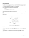
to another is small, the small signal bandwidth of the load limits the minimum transition time for all programmable slew
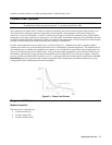
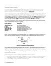
rates. Because of this limitation, the actual transition time is longer than the expected time based on the slew rate, as shown
in Figure 2-8.
Figure 2-8. Risetime Transition Limitation
Therefore, both minimum transition time and slew rate must be considered when determining the actual transition time. This
is shown in Figure 2-9 for the twelve programmable slew rates in current mode operation. The actual transition time will be
either the total slew time (transition divided by slew rate), or the minimum transition time, whichever is longer.
In voltage mode, all minimum transition times are based on a low-capacitance current source. These transition times are
affected by capacitive loading of the inputs. For example, a capacitance of 2.2 microfarads increases the 85 microsecond
minimum transition time (shown in the specifications table) to 110 microseconds. Therefore, no graph is provided for
minimum transition time and slew rate in voltage mode operation.
In resistance mode, the low resistance range uses the slew rate that has been programmed for voltage mode. The middle
resistance range uses the slew rate that has been programmed for the high current range. The high resistance range uses the
slew rate that has been programmed for the low current range.