


Principles of Operation - 4
45
The EEPROM (electrically erasable programmable read-only memory) chip on the A2 interface board
stores a variety of data and configuration information. This information includes calibration constants,
GPIB address, present programming language, and model-dependent data, such as the minimum and
maximum values of voltage and current. One of the EEPROM storage locations holds a checksum value
which is used to verify the integrity of the EEPROM data. Access to the calibration data in the EEPROM is
controlled by the combination of a password and switch settings on A2S201, located on A2 interface board
(See Chapter 3 "Inhibit Calibration Switch").
The Dual 12-bit DAC converts the programmed value of voltage and current on the bus into the CV_Prog
and CC_Prog signals, which are sent to the CV control circuits in order to control the magnitude of the
output voltage in the CV mode and output current in CC mode. The CV_Prog and CC_Prog signals are in
the 0 to -5 V range, which corresponds to the zero to full-scale output ratings of the dc power supply.
The Quad 8-bit DAC converts programmed information for the following circuits into analog format:
overvoltage setting (OV_Prog), and fan speed programming (Fan_Prog). The OV_Prog signal is applied to
the OV detect circuit, which compares the programmed overvoltage setting with the actual output voltage.
The Fan_Prog signal is applied to the fan speed control circuit in order to speed up the fan as temperature
increases, and to slow the fan speed down as temperature decreases.
The 16-bit ADC in conjunction with a 4x1 multiplexer returns data from the following measurement signals
to the logic array: monitored output voltage (VMon), monitored high-range current (Imon_H), monitored
low-range current (Imon_L), and monitored peak current (Imon_P). All measurement signals are in the
range of 0 to +5V, which corresponds to the zero to full-scale readback capability of the dc power supply.
The 8-channel, 8-bit ADC returns the following signals to the logic array: high-range output current
(Imon_H), overvoltage (V_Mon), ambient temperature (Temp_Amb), heatsink temperature (HS_Therm),
and output fuse state (Fuse). Four of these signals are for fan control. The logic array varies the Fan_Prog
signal depending upon the ambient temperature, the heatsink temperature, and the present output voltage
and current. The Fuse signal informs the logic array if the output fuse (F309) is open.
A1 Main Board Circuits
Power Circuits
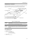
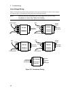
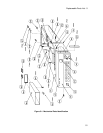
As shown in Figures 6-2 and 6-4, the power circuits consist of: input power rectifiers and filter, primary and
secondary bias circuits, an output regulator, a downprogrammer circuit, current-monitoring resistors, an
overvoltage SCR, and an output filter. All bias circuits are located on the A1 PC board. Bias voltage test
points are shown in Figure 6-1 and transformer wiring diagrams are shown in Figure 3-3.
The primary bias circuits are referenced to chassis (earth) ground. They provide the bias for the GPIB,
RS232 and RI/DFI interfaces, the interface micro-processor circuits and the front panel.
The secondary bias circuits are referenced to secondary (output) common and are isolated from the chassis
ground. They provide the bias for the amplifier and output circuits located on the A1 PC board. They also
provide the bias for the logic array, EEPROM, DAC and ADC circuits and the secondary side of the Opto-
isolators on A2.