


4 - Principles of Operation
44
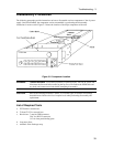
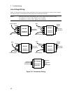
A3 Front Panel Circuits
As shown in Figure 6-3, the supply's front panel assembly contains a circuit board, a keypad, a display, and
a rotary control (RPG) for the output voltage and current. With the exception of the RPG (A3G1), the A3
Front Panel board is an assembly-level replaceable part. A separate front panel binding post board is also
included on the unit. It is also available as an assembly-level replaceable part.
The A3 front panel board contains microprocessor circuits, which decode and execute all keypad and RPG
commands that are transferred to the power supply output via the serial I/O port to the primary interface
circuits on the A2 interface board. The front panel microprocessor circuits also process power supply
measurement and status data received on the serial I/O port and send them to the display.
A2 Interface Circuits
The circuits on the A2 interface board provide the interface between the GPIB interface, RS-232 interface,
and front panel interface and the dc power supply. Communication between the power supply and a GPIB
controller is processed by the GPIB interface and the primary microprocessor circuits on the A2 board. The
A2 Interface board is assembly-level replaceable; it contains no user-replaceable parts.
With the exception of the front panel microprocessor, all digital circuits, analog-to-digital converters (ADC)
and digital-to-analog converters (DAC) in the dc power supply are located on the A2 Interface board.
Control signals between the A2 interface board and the A1 main board are either analog or level signals.
Primary Interface
The primary microprocessor circuits (DSP, ROM, and RAM chips) decode and execute all instructions
and control all data transfers between the controller and the secondary interface. The primary
microprocessor circuits also processes measurement and status data received from the secondary interface.
A Dual Asynchronous Control chip on the A2 board converts the RS-232, RI/DFI, and front panel data into
the primary microprocessor's 8-bit data format. The serial data is transferred between the primary interface
and the secondary interface via a serial bus and optical isolator chips. These chips isolate the primary
interface circuits (referenced to earth ground) from the secondary interface circuits (referenced to the
supply’s output common).
Secondary Interface
The secondary interface circuits include a programmed logic array, EEPROM, boot-ROM, 8 and 12-bit
DAC circuits, and 8 and 16-bit ADC circuits. The programmed logic array translates the serial data
received from the primary interface into a corresponding digital signal for the appropriate DAC/ADC
circuits. The logic array is also connected directly to four DAC/ADC circuits. Under control of the logic
array, the selected DAC converts the data on the bus into an analog signal. Conversely, the selected ADC
converts the analog signals from the A1 board into a digital signal.
The logic array also directly receives status information from the A1 main board via three level-sensitive
signal lines, which inform the array of the following operating conditions: constant voltage mode
(CV_Detect*), constant current mode (CC_Detect*), and overvoltage (OV_Detect*). The PM_Inhibit
control signal is used to shut down the bias voltage to the output stages and keep the power supply output
off. The OV_SCR* control signal is used to fire the SCR and keep the power supply output off when an
overvoltage condition has occurred.