


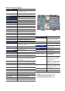
Page 30
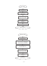
SW2
SW3
SW4
SW5
SW6
SW7
SW8
+
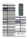
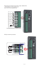
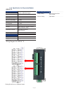
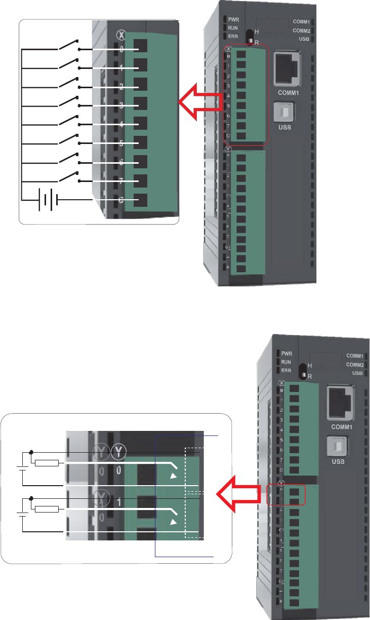
Wiring Diagram for Digital I/Ps and O/Ps of model V288*3S CPU:
1. Wiring diagram for testing digital inputs:
Note: X0 and X1 are high speed input
SW1 X0
X1
X2
X3
X4
X5
X6
F
L
X7
C 0
- 1
24VDC
0
Closing Swx will turn on respective inputs
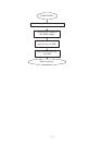
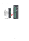
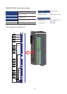
Wiring for transistor type outputs:
Transistor
type O/P
Y1
24VDC
24VDC
LOAD Internal
Circuit
-
F
Y2
L
LOAD Internal
Circuit
0
1
0