


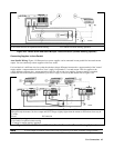

User Connections
60
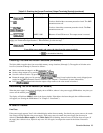
Series 664xA/665xA Power Supplies, Maximum OVP External Capacitance (µF)
6641A 6642A 6643A 6644A 6645A 6651A 6652A 6653A 6654A 6655A
700,000 35,000 15,000 7,000 3,000 1.6 (F) 100,000 50,000 18,000 8,000
If a load capacitance approaches the specified limit, it is recommended that you do not make it a normal practice of tripping
the OVP circuit and discharging the load capacitance through that circuit. This could cause long-term fatigue in some circuit
components.
Because of its high output voltage, the Agilent 6555A generates very high currents when discharging
the load capacitor under overvoltage conditions. Excessive currents can damage the supply. The peak
discharge current is limited by the sum of the external capacitor’s ESR (equivalent series resistance)
and the series resistance of the external circuit. For the Agilent 6555A external capacitance limit of
8,000 µF, this total resistance must be not less than 56 milliohms. For smaller values of external
capacitance, this resistance may be derated linearly.
Inductive Loads
Inductive loads provide no loop stability problems in CV mode. However, in CC mode inductive loads will form a parallel
resonance network with the power supply’s output capacitor. Generally, this will not affect the stability of the supply, but it
may cause ringing of the current in the load. Ringing will not occur if the Q (quality factor) of the parallel resonant network
is ≤ 0.5. Use the following formula to determine the Q of your output.
Q
RR
L
C
int ext
=
+
1
where: C = model-dependent internal capacitance (see below); L = inductance of the load; R
ext
= equivalent series
resistance of the load; R
int
= model-dependent internal resistance (see below):
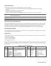
6641A 6642A 6643A 6644A 6645A 6651A 6652A 6653A 6654A 6655A
C =
4,200 µF 550 µF 180 µF 68 µF 33 µF 10,000 µF 1100 µF 440 µF 120 µF 50 µF
R
int
=
7 mΩ 30 mΩ 50 mΩ 125 mΩ 300 mΩ 4 mΩ 20 mΩ 30 mΩ 80 mΩ 250 mΩ
Battery Charging
The power supply’s OVP circuit contains a crowbar SCR that effectively shorts the output of the supply whenever OVP
trips. If a battery (or other external voltage source) is connected across the output and the OVP is inadvertently triggered or
the output is programmed below the battery voltage, the power supply will continuously sink a large current from the
battery. This could damage the supply. To avoid this, insert a reverse blocking diode in series with the
⊕ output of the
supply. Connect the diode cathode to the + battery terminal and the diode anode to the supply
⊕ output terminal. The
diode may require a heat sink.
Note that if the OVP trips, you must remove the external current source in order to reset the internal SCR as part of clearing
the OVP circuit (see Clearing the OV Condition in “Chapter 5 - Front Panel Operation”).
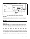
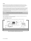
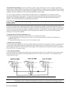
Local Voltage Sensing
Your power supply was shipped set up for local sensing. This means that the supply will sense and regulate its output at the
output terminals, not at the load. Since local sensing does not compensate for voltage drops across screw terminals, bus
bars, or load leads, local sensing should only be used in applications that require low output current or where load regulation
is not critical.
Local sensing is obtained by placing the SENSE switch (see Figure 4-3a) in the Local position. The power supply is
shipped with the switch in this position.