


General Information32
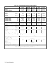
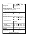
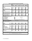
Table 1-3b. Supplemental Characteristics for Series 667xA (continued)
1
Parameter Agilent Model Number
6671A 6672A 6673A 6674A 6675A
Remote Sensing Capability
Voltage Drop Per Lead:
Load Voltage:
Up to 1/2 of rated output voltage.
Subtract voltage drop in load leads from specified output
voltage rating.
Load Regulation:
Degradation due to load lead drop in--output: ∆mV (regulation) = Vdrop(R
sense
-
)/k
Degradation due to load lead drop in + output:
∆mV (regulation) = V
dro
p
(R
sense
+)/k + 2V
dro
p
(V
ratin
g
)/(V
ratin
g
+ 10 V)
where R
sense
- and R
sense
+ are resistances of respective sense leads and k is the following model-dependent
value:
6671A=1; 6672A=1.82; 6673A=4.99; 6674A=10; 6675A=16.2
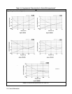
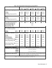
Command Processing Time (Average time for output voltage to change after receipt of digital data when the supply
is connected directly to the GPIB Bus):
20 ms
Output Voltage Programming Response Time**
Rise/Fall Time (time for output to change from 90 % to 10% or from 10% to 90% of its total excursion):***
30 ms
60 ms 130 ms 130 ms 195 ms
Full-load programming speed up/down time (time for output to settle within 4 LSBs of the final value):***
85 ms
190 ms 380 ms 380 ms 600 ms
No-load downprogrammiug discharge time (time for output to fall to 0.5 V when programmed from full voltage to
zero volts):
130 ms
250 ms 350 ms 600 ms 600 ms
** All values exclude command processing time.
*** With full resistive load = V
RATED
/I
RATED.
Monotonicity:
Output is monotonic over entire rated voltage, current, and
temperature range.
Auto-Parallel Configuration:
Up to 3 identical models
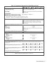
Analog Programming (IP & VP)
Input Signal:*
VP Input Signal:** (0 to )
-4.72 V -4.24 V -4.25 V -4.24 V -3.97 V
VP Input Impedance:
60 kΩ, nominal
IP to -IP Differential Input Signal: (0 to )
+7.79 V +6.81 V +6.81 V =7.01 V +6.34 V
*Signal source must be isolated.
** Referenced to output signal common.
Current Monitor Output (+IM):
Output Signal:* (-0.25 to )
+9.05 V +7.70 V +7.70 V +7.93 v +7.15 V
Output Impedance:
* Corresponds to 0% to 100% output current.
490 Ω
Savable States
Nonvolatile Memory Locations:
Nonvolatile Memory Write Cycles:
Prestored State (factory default):
5 ( 0 through 4)
40,000, typical
Location 0
Notes:
l
For Performance Specifications, see Table l-3a.