


User Connections 59
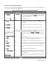
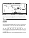
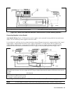
Connecting Series 664xA and 665xA Power Supplies To The Load
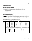
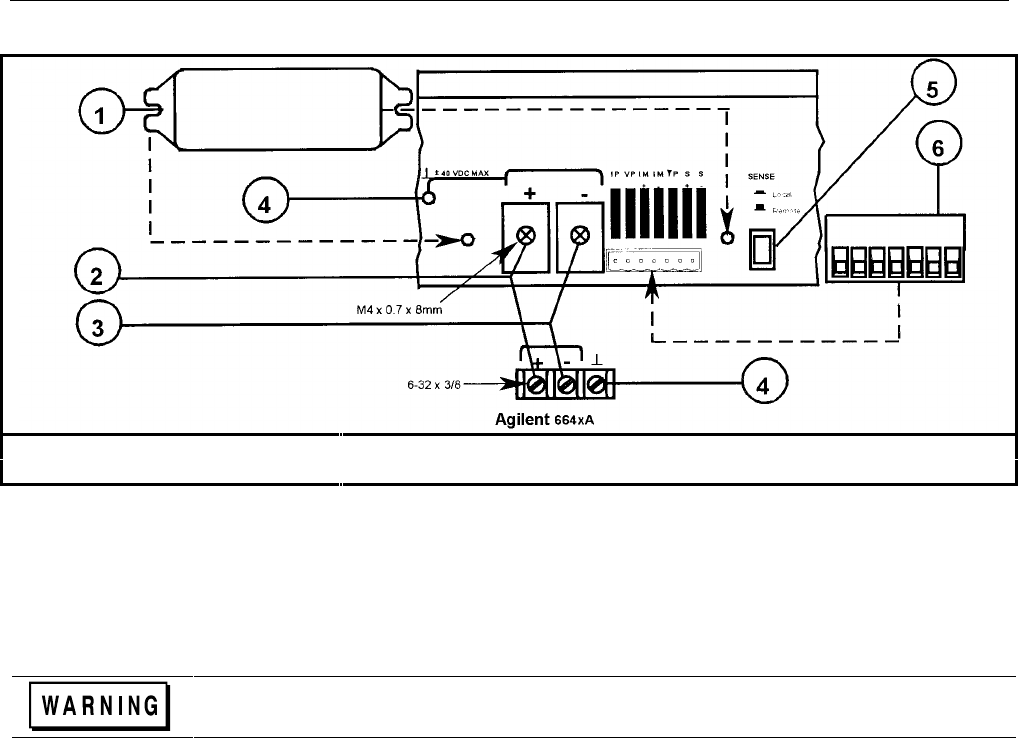
Output Safety Cover ó + Output Terminal ì - Output Terminal
öSignal Common ú Output Sense Switch ÷ Analog Connector
Figure 4-3a. Series 664xA and 665xA Rear Panel Output Connections
Output Isolation
The output of the power supply is isolated from earth ground. Either output terminal may be grounded, or an external
voltage source may be connected between either output and ground. However, both output terminals must be kept within
± 240 Vdc of ground. An earth ground terminal is provided on the rear panel for convenience, such as grounding wire
shields.
The earth ground terminal on the rear panel is a low-noise signal ground for convenience only. It is
not designed to function as a safety ground.
Load Considerations
Capacitive Loads
Effect on the Output Circuit. In most cases, the power supply will continue to be stable with additional external load
capacitors (see the following table for recommendations). However, large load capacitors may cause ringing in the supply’s
transient response. It is possible that certain combinations of load capacitance, equivalent series resistance, and load lead
inductance will result in instability. If you need help in solving a stability problem, contact an Agilent service engineer
through your local Sales and Support Office (see end of this guide).
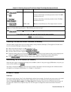
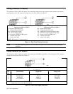
Series 664xA/665xA Power Supplies, Maximum External Capacitance (µF)
6641A 6642A 6643A 6644A 6645A 6651A 6652A 6653A 6654A 6655A
40,000 20,000 12,000 7,000 3,000 100,000 50,000 30,000 18,000 8,000
If the power supply output is rapidly programmed into capacitive loads, the supply may momentarily cross into CC mode.
This extends the CV programming time and limits the maximum slew rate to the programmed current divided by the total
internal (see the following section “Inductive Loads”) and external capacitance. These momentary crossovers into CC mode
will not damage the supply.
Effect on the OVP Circuit. The OVP circuit is designed to discharge fully-charged capacitances up to a specified limit for
each model. These limits are as follows: